Our Products
Comprehensive industrial automation solutions for global industries
Contact us
If you are interested in our products and want to know more details,please Contact us,we will reply you as soon as we can.
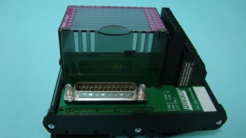
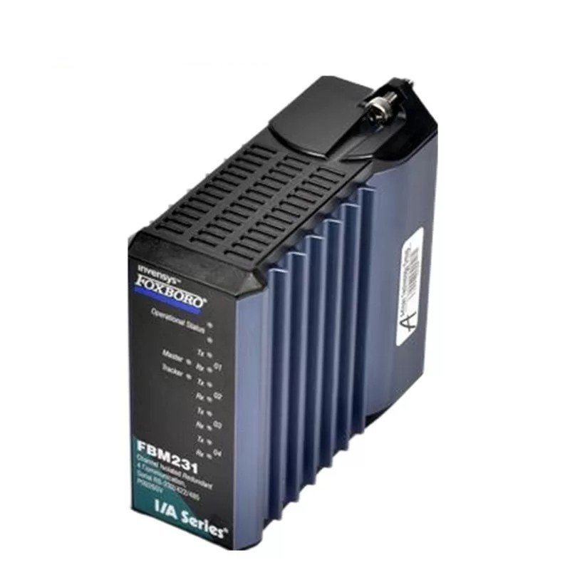
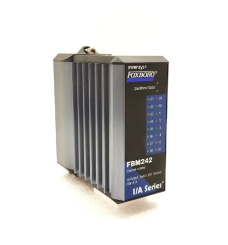
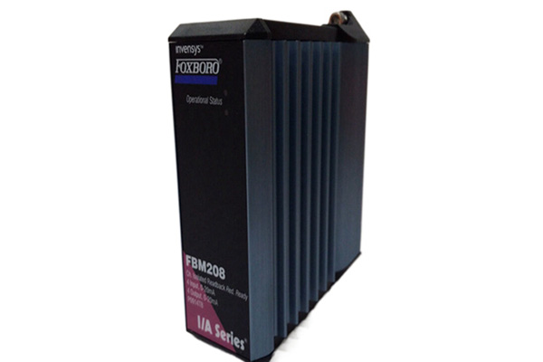
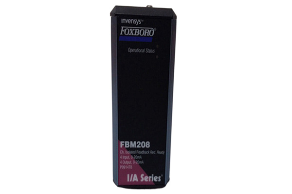
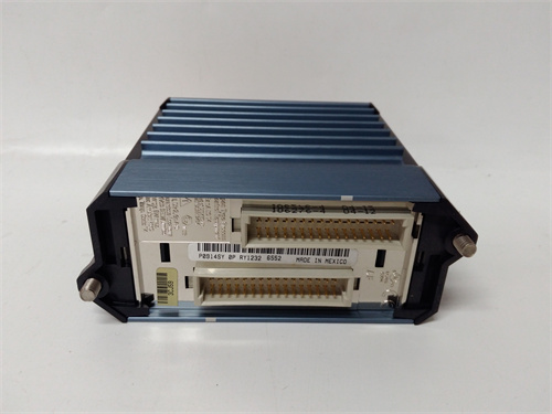
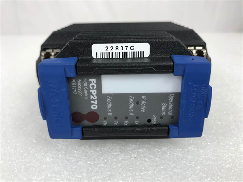
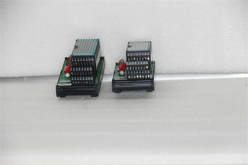
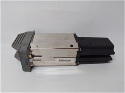
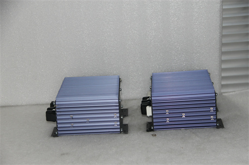
Foxboro FBM208 P0914TB Critical Area Analysis Module
Module Number:FBM208 P0914TB
Product status:Discontinued
Delivery time:In stock
Sales country:All over the world
Product situation:Brandnew , one year warranty
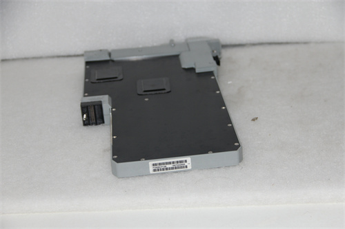
Product Description
The FBM208 P0914TB area is a layout area where certain sized particles can cause a functional failure, depending solely on the layout to be simulated and the size range of the particles. The critical area analysis will calculate the expected average number of failures and yield rate based on the size and spacing of layout features, particle size, and density distribution measured by the wafer factory. In addition to traditional short-circuit and open circuit calculations, the work currently being done in critical area analysis also includes through-hole and contact faults. These analyses typically indicate that via and contact faults are the main fault mechanisms. Other fault mechanisms can also be included in the analysis, depending on the defect data provided by the wafer factory.
The FBM208 P0914TB area will increase as the size of defects or particles increases. For extreme cases where the defect size is large enough, the entire chip area is a critical area. However, in reality, most wafer fabs limit the range of defect sizes that can be simulated based on the defect size range that can be detected and measured by the test chip or measuring equipment.
 Loading comments...
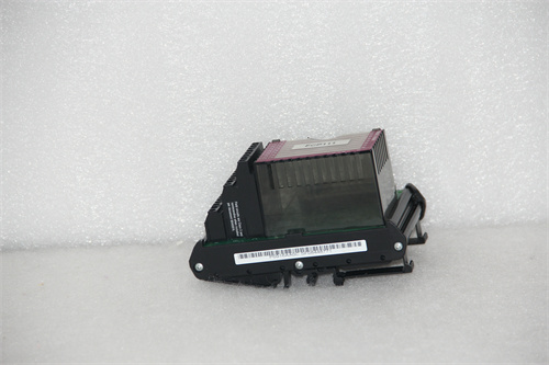
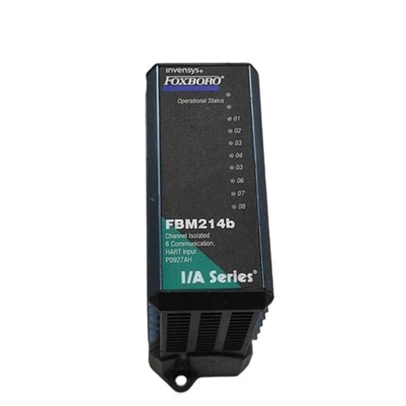
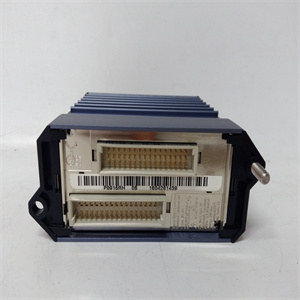
Foxboro FBM208 P0914TB Critical Area Analysis Module
Module Number:FBM208 P0914TB
Product status:Discontinued
Delivery time:In stock
Sales country:All over the world
Product situation:Brandnew , one year warranty
Product Description
The FBM208 P0914TB area is a layout area where certain sized particles can cause a functional failure, depending solely on the layout to be simulated and the size range of the particles. The critical area analysis will calculate the expected average number of failures and yield rate based on the size and spacing of layout features, particle size, and density distribution measured by the wafer factory. In addition to traditional short-circuit and open circuit calculations, the work currently being done in critical area analysis also includes through-hole and contact faults. These analyses typically indicate that via and contact faults are the main fault mechanisms. Other fault mechanisms can also be included in the analysis, depending on the defect data provided by the wafer factory.
The FBM208 P0914TB area will increase as the size of defects or particles increases. For extreme cases where the defect size is large enough, the entire chip area is a critical area. However, in reality, most wafer fabs limit the range of defect sizes that can be simulated based on the defect size range that can be detected and measured by the test chip or measuring equipment.
Need a Custom Automation Solution?
Our team of experts can design and implement a tailored automation system to meet your specific requirements.