Our Products
Comprehensive industrial automation solutions for global industries
Contact us
If you are interested in our products and want to know more details,please Contact us,we will reply you as soon as we can.
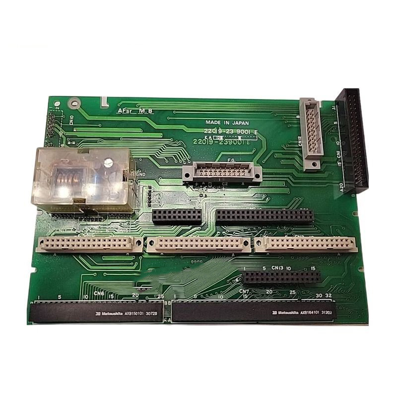
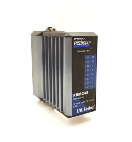
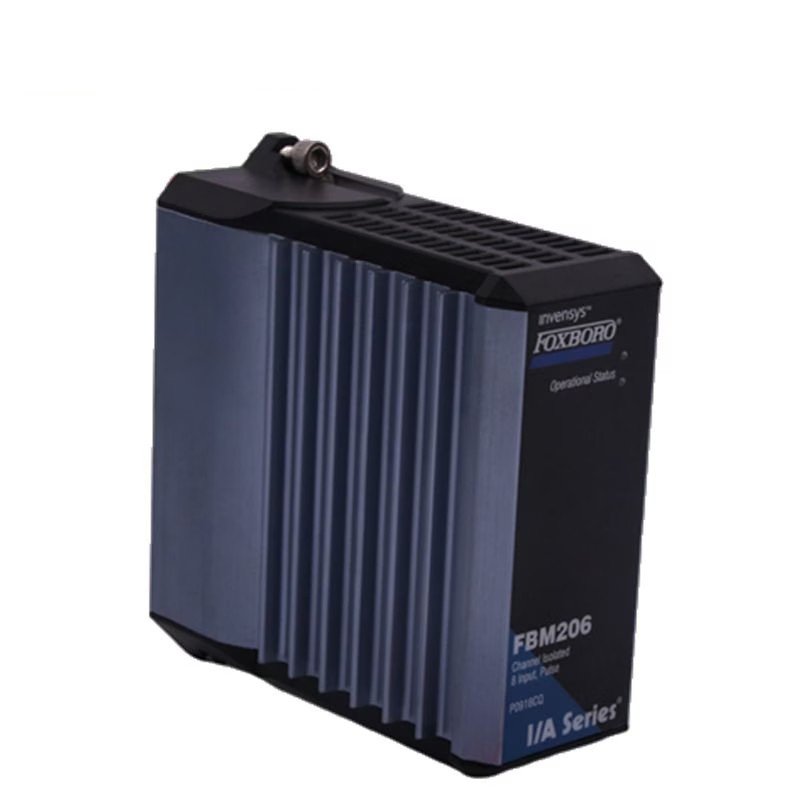
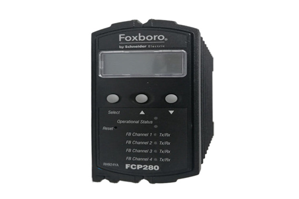
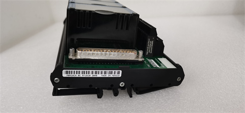
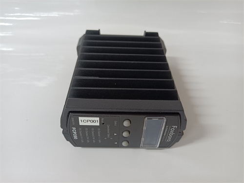
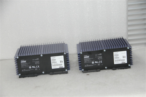
Foxboro FCP280 RH924YA Wireless Transceiver Module
Module Number:FCP280 RH924YA
Product staus:Discontinued
Delivery time:In stock
Sales country:All over the world
Product situation:Brandnew , one year warranty
Product Size:250*235*85mm
Product Weight:2.5 kg
Power withstand :3.5 KVA
Product Description
The home FCP280 RH924YA is the core component of embedded smart home systems, and the designed wireless transceiver module circuit is a part of the home gateway. The principle and design method of a wireless transceiver module circuit composed of a single RF transceiver chip nRF0433. The designed wireless transceiver module circuit operates in the 433MHz ISM frequency band, with a data rate of 9600bit/s, a high sensitivity of -105dBm, a maximum transmission power of 10mW, a power supply voltage of 215-515V, and a working current of 31-47mA.
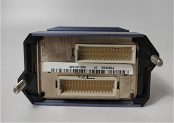
Antenna input/output, when nRF0433 is in receive mode, the ANT1 (pin 16) and ANT2 (pin 15) pins provide RF input to the low-noise amplifier LNA; When nRF0433 is in transmission mode, RF output is provided from the power amplifier to the antenna. The antenna is connected to nRF0433 in differential form, and the recommended load impedance in the antenna channel is 400 Ω.
The differential FCP280 RH924YA antenna on the printed circuit board (PCB) is shown in the application circuit printed circuit board diagram. The output stage of the power amplifier consists of two transistors with open collector electrodes in a differential structure, and the power supply VDD to the power amplifier must be supplied through the collector load. When connecting the differential loop antenna to the ANT1/ANT2 pin end, the power VDD will be supplied through the center of the loop antenna. When connecting a single ended antenna to FCP280 RH924YA, use differential to single ended matching network. A single ended antenna can also be connected to nRF0433 using an 8:1 RF transformer, operating at 433MHz. The primary side of the RF transformer must have a central tap for VDD power supply. Set the output power of resistor R3 connected between RF-PWR (pin 11) and+5V.
 Loading comments...
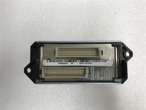
Foxboro FCP280 RH924YA Wireless Transceiver Module
Module Number:FCP280 RH924YA
Product staus:Discontinued
Delivery time:In stock
Sales country:All over the world
Product situation:Brandnew , one year warranty
Product Size:250*235*85mm
Product Weight:2.5 kg
Power withstand :3.5 KVA
Product Description
The home FCP280 RH924YA is the core component of embedded smart home systems, and the designed wireless transceiver module circuit is a part of the home gateway. The principle and design method of a wireless transceiver module circuit composed of a single RF transceiver chip nRF0433. The designed wireless transceiver module circuit operates in the 433MHz ISM frequency band, with a data rate of 9600bit/s, a high sensitivity of -105dBm, a maximum transmission power of 10mW, a power supply voltage of 215-515V, and a working current of 31-47mA.
Antenna input/output, when nRF0433 is in receive mode, the ANT1 (pin 16) and ANT2 (pin 15) pins provide RF input to the low-noise amplifier LNA; When nRF0433 is in transmission mode, RF output is provided from the power amplifier to the antenna. The antenna is connected to nRF0433 in differential form, and the recommended load impedance in the antenna channel is 400 Ω.
The differential FCP280 RH924YA antenna on the printed circuit board (PCB) is shown in the application circuit printed circuit board diagram. The output stage of the power amplifier consists of two transistors with open collector electrodes in a differential structure, and the power supply VDD to the power amplifier must be supplied through the collector load. When connecting the differential loop antenna to the ANT1/ANT2 pin end, the power VDD will be supplied through the center of the loop antenna. When connecting a single ended antenna to FCP280 RH924YA, use differential to single ended matching network. A single ended antenna can also be connected to nRF0433 using an 8:1 RF transformer, operating at 433MHz. The primary side of the RF transformer must have a central tap for VDD power supply. Set the output power of resistor R3 connected between RF-PWR (pin 11) and+5V.
Need a Custom Automation Solution?
Our team of experts can design and implement a tailored automation system to meet your specific requirements.