Our Products
Comprehensive industrial automation solutions for global industries
Contact us
If you are interested in our products and want to know more details,please Contact us,we will reply you as soon as we can.
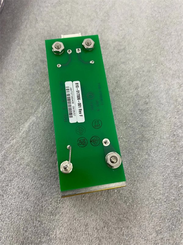
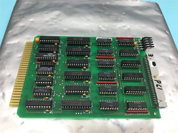
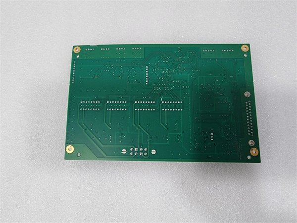
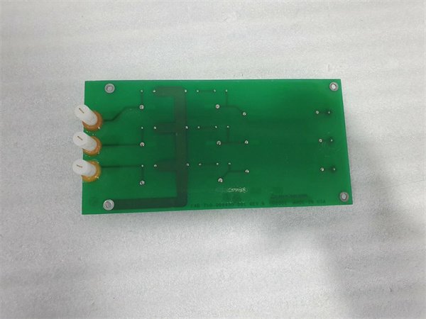
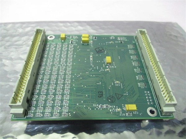
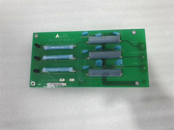
LAM 715-003851-002 Optical Wafer Inspection Interface Module
Manufacturer: LAM Research
Product Number: 715-003851-002
Category: Optical Wafer Inspection Interface Module
Application: Semiconductor wafer quality control platforms requiring high-performance optical inspection interface
Product Description
The 715-003851-002 is a high-performance optical wafer inspection interface module developed by LAM Research, a global leader in semiconductor manufacturing equipment. Explicitly engineered for integration into LAM’s wafer quality control platforms—including the Centura® Wafer Inspection System, Sym3® Film Quality Monitor, and Versys® Defect Review Tool—this module serves as the “signal processing hub” for translating raw optical data from inspection sensors into actionable quality control insights.
As a flagship model in LAM’s Optical Inspection Series, the 715-003851-002 is optimized for advanced semiconductor process nodes (down to 3nm), where nanoscale defects (e.g., 50nm particle contamination, 10nm film thickness variations) can render entire wafers non-functional. Its core function is to receive, process, and enhance signals from high-resolution inspection sensors—such as 12MP defect cameras and surface profilometers—then transmit processed data to the main control system or defect review software. In automation systems, the 715-003851-002 acts as a critical link between inspection hardware and subsystems like the 810-01915-003 robotic wafer handling module—triggering wafer repositioning or rejection based on real-time defect detection, directly improving overall fab yield.
Detailed Parameter Table
| Parameter Name | Parameter Value |
| Product model | 715-003851-002 |
| Manufacturer | LAM Research |
| Product category | Optical Wafer Inspection Interface Module (for Semiconductor Wafer Quality Control) |
| Sensor Compatibility | High-resolution defect cameras (up to 12MP), surface profilometers, film thickness sensors (ellipsometers/spectrometers) |
| Input Channels | 2x high-speed analog video inputs (12-bit, 4K@60fps); 4x digital sensor inputs (TTL/RS-422) |
| Output Signals | 2x processed video outputs (HDMI 2.0, 4K@60fps); 3x digital trigger outputs (24V DC, sinking) |
| Signal Processing Speed | 1.2 GB/s (analog video data throughput); 500μs (defect detection signal latency) |
| Interface Type | Dual Ethernet (10/100/1000Base-T); RS-485; 2x 28-pin terminal blocks (power/sensor signals); 1x USB-C (configuration); 1x SFP+ (for high-speed data transfer) |
| Communication Protocol | EtherNet/IP, Modbus TCP/IP, LAM Proprietary InspectLink™ v3.0 |
| Operating Temperature Range | 10°C to 40°C (non-condensing) |
| Relative Humidity Tolerance | 15% to 75% RH (non-condensing, no moisture ingress) |
| Physical Dimensions (W×H×D) | 190mm × 250mm × 100mm (excluding connectors/terminal blocks) |
| Installation Method | DIN rail mounting (35mm standard); panel mounting (with low-profile, anti-vibration brackets) |
| Certifications | CE, UL 61010-1, SEMI S2/S8/S14 (semiconductor safety/EMC/image quality standards) |
| Power Consumption | 24V DC, 1.5A typical; 2.2A maximum (all channels active, video processing enabled) |
| Image Enhancement Features | Real-time noise reduction, edge sharpening, defect contrast enhancement (configurable via software) |
| Calibration Support | NIST-traceable optical reference calibration; software-guided sensor alignment wizard |
Core Advantages and Technical Highlights
Ultra-High-Speed Signal Processing for Nanoscale Defect Detection: The 715-003851-002 delivers a data throughput of 1.2 GB/s and a signal latency of <500μs—far exceeding legacy inspection interfaces (typically 500 MB/s, 2ms latency)—enabling real-time detection of sub-100nm defects. This speed is enabled by a dedicated FPGA (Field-Programmable Gate Array) for video processing and a multi-core processor for defect analysis. For 3nm logic wafers, this means the module can identify tiny surface scratches or particle contamination while the wafer is still in the inspection tool, allowing for immediate rework or rejection before the wafer proceeds to costly etching or deposition steps.
Advanced Image Enhancement and Sensor Versatility: Unlike basic inspection interfaces that only pass raw sensor data, the 715-003851-002 includes built-in image enhancement tools—real-time noise reduction, edge sharpening, and contrast adjustment—that improve defect visibility in low-light or high-reflection conditions (e.g., metal-layer wafer surfaces). It also supports multiple sensor types (defect cameras, profilometers, ellipsometers), eliminating the need for separate interface modules for different inspection tasks. For example, it can simultaneously process 4K video from a defect camera and thickness data from an ellipsometer, correlating surface defects with film thickness variations to identify root causes (e.g., uneven deposition leading to particle adhesion).
Semiconductor-Grade Optical Integrity and Durability: Built to SEMI S2/S8/S14 standards, the 715-003851-002 features a light-shielded housing that blocks ambient light interference (critical for high-sensitivity imaging) and conformal-coated circuit boards that resist corrosion from low-level process gas leaks (e.g., ammonia, fluorine). Its high-speed video inputs/outputs use shielded cables to minimize EMI (electromagnetic interference) from nearby tools like the 810-069751-114 plasma impedance module, ensuring image data remains free of artifacts. The module’s mean time between failures (MTBF) exceeds 180,000 hours, ensuring reliable operation in 24/7 inspection lines.
Seamless Integration with Automation Workflows: Equipped with LAM’s InspectLink™ v3.0 protocol, the 715-003851-002 synchronizes inspection data with other fab systems. When it detects a defect above the acceptable threshold, it sends a trigger signal to the 810-01915-003 robotic module to reroute the wafer to a defect review station, while logging the defect’s coordinates, size, and type to LAM’s FabGuard® analytics platform. This integration reduces manual intervention by 40% compared to legacy systems, accelerating defect analysis and minimizing the risk of defective wafers entering subsequent processes.
Typical Application Scenarios
The 715-003851-002 is indispensable in semiconductor fabs for quality control operations, with two high-impact use cases: post-etch defect inspection for 3nm logic wafers and pre-deposition surface quality checks for 3D NAND wafers.
In post-etch defect inspection (e.g., LAM’s Centura® Wafer Inspection System), the 715-003851-002 processes 4K video from a 12MP top-down defect camera to identify etch-related defects like line-edge roughness, missing features, or residual polymer. Its real-time edge sharpening enhances the visibility of sub-50nm line-edge variations, while its low latency ensures the 810-01915-003 robot can reject defective wafers within 1 second of inspection. Fabs using the 715-003851-002 report a 32% reduction in escaped defects (defects not detected until later processes), which saves significant costs by avoiding wasted deposition or metallization on faulty wafers.
In pre-deposition surface quality checks (e.g., Sym3® Film Quality Monitor for 3D NAND), the 715-003851-002 integrates data from a surface profilometer and a particle detection camera. It checks for surface flatness (ensuring <5nm variation across 300mm wafers) and particle contamination (<10 particles >50nm), critical for uniform CVD deposition. If it detects a high particle count, it triggers a cleaning cycle in the upstream wafer handling tool, preventing the particles from causing voids in the 3D NAND’s dielectric layers. The module’s ability to correlate profilometer and camera data also helps engineers identify issues like uneven wafer handling (causing scratches) or contaminated robot end effectors (causing particle transfer).
Installation Commissioning and Maintenance Instructions
Installation Preparation: Before installing the 715-003851-002, ensure the mounting surface (DIN rail/panel) is clean (Class 1 cleanroom compliant) and ambient temperature is 10–40°C. Required tools include a torque screwdriver (0.6 N·m for DIN rail mounting), light meter (to verify ambient light levels <10 lux), ESD-safe gloves/wristbands, and a laptop (for USB-C configuration). Safety precautions: Disconnect power to the host inspection system before wiring; use shielded, twisted-pair cables for video inputs/outputs to minimize EMI; confirm the module’s ground connection (≥12AWG wire) is secure to prevent ESD damage. Avoid mounting near light sources (e.g., inspection tool LEDs) or high-voltage components to prevent optical or electrical interference.
Maintenance Suggestions: For daily maintenance, check the 715-003851-002’s front-panel LED indicators (green = normal, amber = signal warning, red = critical fault) and verify image quality via InspectLink™ software. Every 3 months, clean the module’s light-shielded housing with a lint-free cloth (avoid liquids) and check video cables for wear (replace if signal artifacts appear). Every 12 months, perform a calibration using the LAM 715-003854-002 accessory to verify defect detection accuracy; update the module’s firmware via Ethernet to access new image enhancement features. If a fault occurs (e.g., video signal loss), first check sensor wiring and cable connections, then use the module’s diagnostic tool to isolate the issue—never open the light-shielded housing, as internal components are sensitive to ambient light and require factory servicing.
 Loading comments...
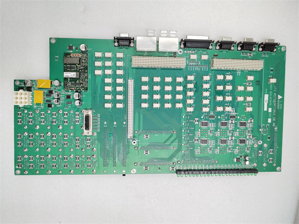
LAM 715-003851-002 Optical Wafer Inspection Interface Module
Manufacturer: LAM Research
Product Number: 715-003851-002
Category: Optical Wafer Inspection Interface Module
Application: Semiconductor wafer quality control platforms requiring high-performance optical inspection interface
Product Description
The 715-003851-002 is a high-performance optical wafer inspection interface module developed by LAM Research, a global leader in semiconductor manufacturing equipment. Explicitly engineered for integration into LAM’s wafer quality control platforms—including the Centura® Wafer Inspection System, Sym3® Film Quality Monitor, and Versys® Defect Review Tool—this module serves as the “signal processing hub” for translating raw optical data from inspection sensors into actionable quality control insights.
As a flagship model in LAM’s Optical Inspection Series, the 715-003851-002 is optimized for advanced semiconductor process nodes (down to 3nm), where nanoscale defects (e.g., 50nm particle contamination, 10nm film thickness variations) can render entire wafers non-functional. Its core function is to receive, process, and enhance signals from high-resolution inspection sensors—such as 12MP defect cameras and surface profilometers—then transmit processed data to the main control system or defect review software. In automation systems, the 715-003851-002 acts as a critical link between inspection hardware and subsystems like the 810-01915-003 robotic wafer handling module—triggering wafer repositioning or rejection based on real-time defect detection, directly improving overall fab yield.
Detailed Parameter Table
| Parameter Name | Parameter Value |
| Product model | 715-003851-002 |
| Manufacturer | LAM Research |
| Product category | Optical Wafer Inspection Interface Module (for Semiconductor Wafer Quality Control) |
| Sensor Compatibility | High-resolution defect cameras (up to 12MP), surface profilometers, film thickness sensors (ellipsometers/spectrometers) |
| Input Channels | 2x high-speed analog video inputs (12-bit, 4K@60fps); 4x digital sensor inputs (TTL/RS-422) |
| Output Signals | 2x processed video outputs (HDMI 2.0, 4K@60fps); 3x digital trigger outputs (24V DC, sinking) |
| Signal Processing Speed | 1.2 GB/s (analog video data throughput); 500μs (defect detection signal latency) |
| Interface Type | Dual Ethernet (10/100/1000Base-T); RS-485; 2x 28-pin terminal blocks (power/sensor signals); 1x USB-C (configuration); 1x SFP+ (for high-speed data transfer) |
| Communication Protocol | EtherNet/IP, Modbus TCP/IP, LAM Proprietary InspectLink™ v3.0 |
| Operating Temperature Range | 10°C to 40°C (non-condensing) |
| Relative Humidity Tolerance | 15% to 75% RH (non-condensing, no moisture ingress) |
| Physical Dimensions (W×H×D) | 190mm × 250mm × 100mm (excluding connectors/terminal blocks) |
| Installation Method | DIN rail mounting (35mm standard); panel mounting (with low-profile, anti-vibration brackets) |
| Certifications | CE, UL 61010-1, SEMI S2/S8/S14 (semiconductor safety/EMC/image quality standards) |
| Power Consumption | 24V DC, 1.5A typical; 2.2A maximum (all channels active, video processing enabled) |
| Image Enhancement Features | Real-time noise reduction, edge sharpening, defect contrast enhancement (configurable via software) |
| Calibration Support | NIST-traceable optical reference calibration; software-guided sensor alignment wizard |
Core Advantages and Technical Highlights
Ultra-High-Speed Signal Processing for Nanoscale Defect Detection: The 715-003851-002 delivers a data throughput of 1.2 GB/s and a signal latency of <500μs—far exceeding legacy inspection interfaces (typically 500 MB/s, 2ms latency)—enabling real-time detection of sub-100nm defects. This speed is enabled by a dedicated FPGA (Field-Programmable Gate Array) for video processing and a multi-core processor for defect analysis. For 3nm logic wafers, this means the module can identify tiny surface scratches or particle contamination while the wafer is still in the inspection tool, allowing for immediate rework or rejection before the wafer proceeds to costly etching or deposition steps.
Advanced Image Enhancement and Sensor Versatility: Unlike basic inspection interfaces that only pass raw sensor data, the 715-003851-002 includes built-in image enhancement tools—real-time noise reduction, edge sharpening, and contrast adjustment—that improve defect visibility in low-light or high-reflection conditions (e.g., metal-layer wafer surfaces). It also supports multiple sensor types (defect cameras, profilometers, ellipsometers), eliminating the need for separate interface modules for different inspection tasks. For example, it can simultaneously process 4K video from a defect camera and thickness data from an ellipsometer, correlating surface defects with film thickness variations to identify root causes (e.g., uneven deposition leading to particle adhesion).
Semiconductor-Grade Optical Integrity and Durability: Built to SEMI S2/S8/S14 standards, the 715-003851-002 features a light-shielded housing that blocks ambient light interference (critical for high-sensitivity imaging) and conformal-coated circuit boards that resist corrosion from low-level process gas leaks (e.g., ammonia, fluorine). Its high-speed video inputs/outputs use shielded cables to minimize EMI (electromagnetic interference) from nearby tools like the 810-069751-114 plasma impedance module, ensuring image data remains free of artifacts. The module’s mean time between failures (MTBF) exceeds 180,000 hours, ensuring reliable operation in 24/7 inspection lines.
Seamless Integration with Automation Workflows: Equipped with LAM’s InspectLink™ v3.0 protocol, the 715-003851-002 synchronizes inspection data with other fab systems. When it detects a defect above the acceptable threshold, it sends a trigger signal to the 810-01915-003 robotic module to reroute the wafer to a defect review station, while logging the defect’s coordinates, size, and type to LAM’s FabGuard® analytics platform. This integration reduces manual intervention by 40% compared to legacy systems, accelerating defect analysis and minimizing the risk of defective wafers entering subsequent processes.
Typical Application Scenarios
The 715-003851-002 is indispensable in semiconductor fabs for quality control operations, with two high-impact use cases: post-etch defect inspection for 3nm logic wafers and pre-deposition surface quality checks for 3D NAND wafers.
In post-etch defect inspection (e.g., LAM’s Centura® Wafer Inspection System), the 715-003851-002 processes 4K video from a 12MP top-down defect camera to identify etch-related defects like line-edge roughness, missing features, or residual polymer. Its real-time edge sharpening enhances the visibility of sub-50nm line-edge variations, while its low latency ensures the 810-01915-003 robot can reject defective wafers within 1 second of inspection. Fabs using the 715-003851-002 report a 32% reduction in escaped defects (defects not detected until later processes), which saves significant costs by avoiding wasted deposition or metallization on faulty wafers.
In pre-deposition surface quality checks (e.g., Sym3® Film Quality Monitor for 3D NAND), the 715-003851-002 integrates data from a surface profilometer and a particle detection camera. It checks for surface flatness (ensuring <5nm variation across 300mm wafers) and particle contamination (<10 particles >50nm), critical for uniform CVD deposition. If it detects a high particle count, it triggers a cleaning cycle in the upstream wafer handling tool, preventing the particles from causing voids in the 3D NAND’s dielectric layers. The module’s ability to correlate profilometer and camera data also helps engineers identify issues like uneven wafer handling (causing scratches) or contaminated robot end effectors (causing particle transfer).
Installation Commissioning and Maintenance Instructions
Installation Preparation: Before installing the 715-003851-002, ensure the mounting surface (DIN rail/panel) is clean (Class 1 cleanroom compliant) and ambient temperature is 10–40°C. Required tools include a torque screwdriver (0.6 N·m for DIN rail mounting), light meter (to verify ambient light levels <10 lux), ESD-safe gloves/wristbands, and a laptop (for USB-C configuration). Safety precautions: Disconnect power to the host inspection system before wiring; use shielded, twisted-pair cables for video inputs/outputs to minimize EMI; confirm the module’s ground connection (≥12AWG wire) is secure to prevent ESD damage. Avoid mounting near light sources (e.g., inspection tool LEDs) or high-voltage components to prevent optical or electrical interference.
Maintenance Suggestions: For daily maintenance, check the 715-003851-002’s front-panel LED indicators (green = normal, amber = signal warning, red = critical fault) and verify image quality via InspectLink™ software. Every 3 months, clean the module’s light-shielded housing with a lint-free cloth (avoid liquids) and check video cables for wear (replace if signal artifacts appear). Every 12 months, perform a calibration using the LAM 715-003854-002 accessory to verify defect detection accuracy; update the module’s firmware via Ethernet to access new image enhancement features. If a fault occurs (e.g., video signal loss), first check sensor wiring and cable connections, then use the module’s diagnostic tool to isolate the issue—never open the light-shielded housing, as internal components are sensitive to ambient light and require factory servicing.
Need a Custom Automation Solution?
Our team of experts can design and implement a tailored automation system to meet your specific requirements.