Our Products
Comprehensive industrial automation solutions for global industries
Contact us
If you are interested in our products and want to know more details,please Contact us,we will reply you as soon as we can.
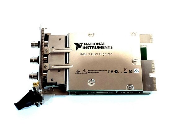
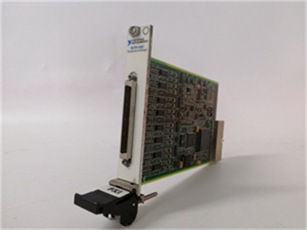
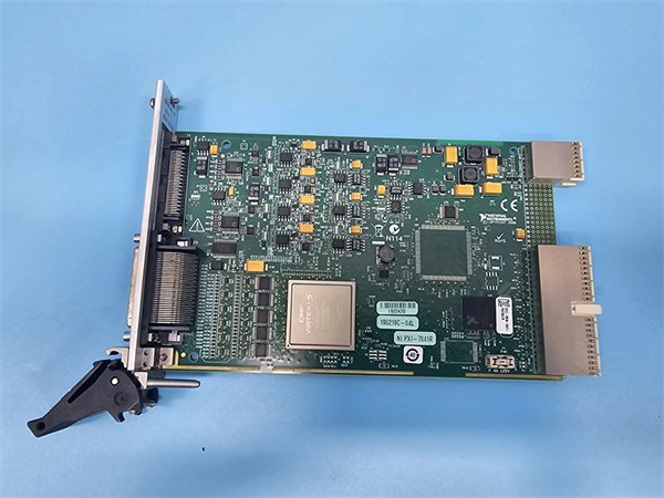
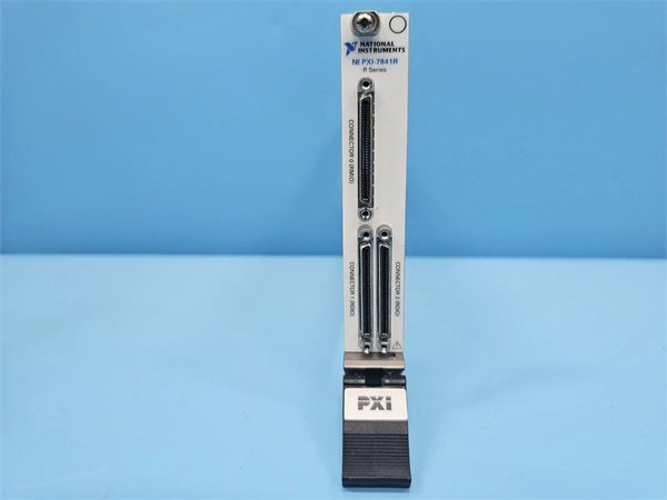
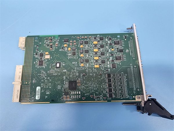
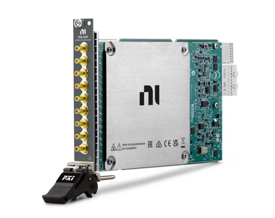
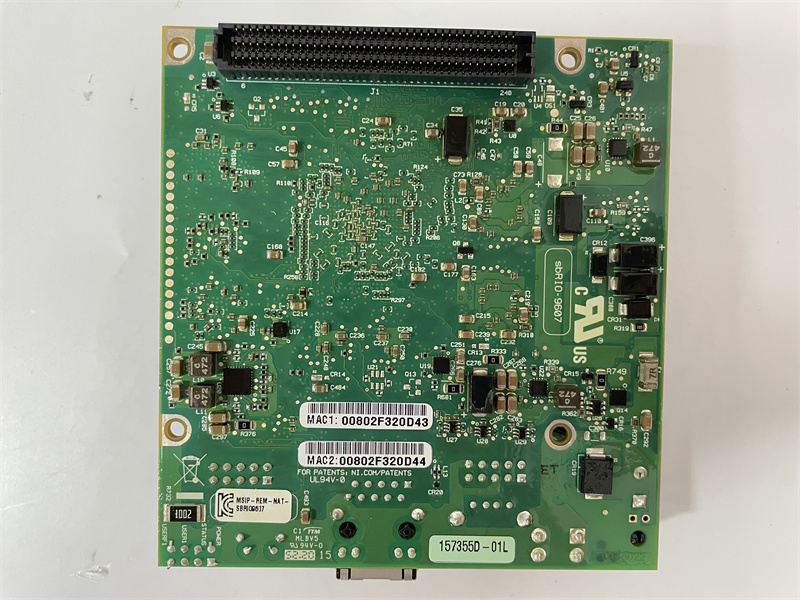
NI PXIE-7846 FPGA-Based Reconfigurable I/O Module
Manufacturer: National Instruments (NI)
Product Number: PXIe-7846
Category: FPGA-Based Reconfigurable I/O Module (PXIe)
FPGA: Xilinx Kintex-7
Analog Inputs: 8 (16-bit, 750 kS/s)
Analog Outputs: 8 (16-bit, 1 MS/s)
Digital I/O: 48 (3.3 V or 5 V configurable)
Form Factor: 3U PXIe
Operating Temperature: 0°C to +55°C
Product Description
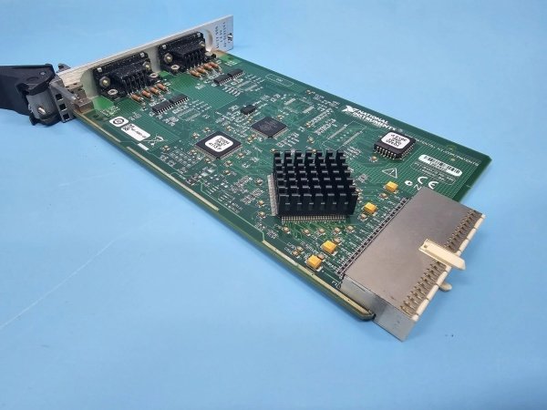
The NI PXIE-7846 is a high-performance FPGA-based reconfigurable I/O module designed for PXIe systems, combining the flexibility of field-programmable gate arrays (FPGAs) with integrated analog and digital I/O for custom test, measurement, and control applications. As part of NI’s R Series, it empowers engineers to implement specialized hardware logic directly on the FPGA, enabling low-latency, deterministic operations tailored to unique application requirements.
Featuring a Xilinx Kintex-7 160T FPGA, the NI PXIE-7846 delivers exceptional processing power with 2,757 DSP slices and over 1.5 million logic cells, supporting complex algorithms like real-time signal processing and custom protocol implementation. Its 16 analog input channels (250 kS/s simultaneous sampling) and 4 analog outputs (1 MS/s) provide versatile signal acquisition and generation, while 96 digital I/O lines offer extensive connectivity for digital control tasks. In automated test systems, the NI PXIE-7846 acts as a customizable core, adapting to evolving test requirements without hardware redesign—from high-speed data logging to closed-loop control with microsecond-level response times.
Detailed Parameter Table
| Parameter Name | Parameter Value |
| Product Model | PXIE-7846 |
| Manufacturer | National Instruments (NI) |
| Product Category | FPGA-Based Reconfigurable I/O Module for PXIe Systems |
| FPGA Chip | Xilinx Kintex-7 160T (2,757 DSP slices, 1,585,536 logic cells) |
| Analog Input Channels | 16 (16-bit, 250 kS/s per channel, simultaneous sampling) |
| Analog Input Ranges | ±10 V, ±5 V, ±2.5 V, ±1 V, ±500 mV, ±250 mV, ±100 mV, ±50 mV |
| Analog Output Channels | 4 (16-bit, 1 MS/s per channel) |
| Analog Output Ranges | ±10 V, 0-10 V |
| Digital I/O Lines | 96 (configurable as input, output, or special functions; 3.3 V/5 V tolerant) |
| Counter/Timers | 4 (32-bit, 80 MHz) integrated in FPGA, expandable via digital lines |
| Memory | 1 GB DDR3 SDRAM (1600 MHz) |
| Interface | PXI Express (x4 lane, Gen 2) |
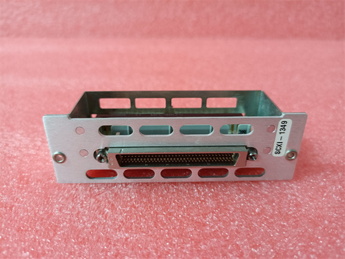
| Connector Type | 2 x 68-pin VHDCI (analog I/O), 1 x 100-pin SCSI (digital I/O) |
| Operating Temperature Range | 0 °C to 55 °C |
| Power Consumption | 25 W typical |
| Physical Dimensions | 16.8 cm x 10.0 cm (length x width) |
| Weight | 1.1 kg |
| Software Compatibility | LabVIEW FPGA Module, LabVIEW Real-Time Module, NI-DAQmx, C/C++ (with FPGA Interface C API) |
| Calibration Interval | 1 year |
Core Advantages and Technical Highlights
Reconfigurable FPGA Architecture: The Xilinx Kintex-7 160T FPGA in the NI PXIE-7846 enables full customization of hardware behavior. Engineers can implement custom triggers, protocol decoders (e.g., CAN, Ethernet), or real-time filters directly on the FPGA, eliminating the latency of software-based processing. This flexibility is invaluable in applications like aerospace radar testing, where unique signal processing algorithms are required.
Synchronized Mixed-Signal I/O: With 16 simultaneous-sampling analog inputs and 4 high-speed analog outputs, the NI PXIE-7846 ensures precise timing alignment across all channels. Combined with 96 digital I/O lines, it supports mixed-signal test scenarios—for example, generating analog stimuli, measuring responses, and toggling digital control signals in lockstep, critical for validating complex electronic systems.
High-Performance Processing: The FPGA’s 2,757 DSP slices and 1 GB DDR3 SDRAM enable the NI PXIE-7846 to handle intensive tasks like FFTs, digital filtering, and PID control in hardware. This processing power, paired with the x4 Gen 2 PXIe interface (8 GB/s bandwidth), allows for high-throughput data transfer between the FPGA and host, ideal for applications requiring real-time analysis of large datasets.
Scalable Digital Functionality: The 96 digital I/O lines are configurable as general-purpose I/O, counters, or custom protocol interfaces (e.g., SPI, I2C, UART). This scalability lets the NI PXIE-7846 adapt to diverse digital test needs, from simulating sensors with custom timing to emulating communication buses in embedded system validation.
Typical Application Scenarios
Aerospace and Defense Test: In avionics testing, the NI PXIE-7846 emulates complex sensor suites (gyroscopes, accelerometers) by generating synchronized analog and digital signals. Its FPGA implements custom error-checking logic for MIL-STD protocols, validating that flight control systems respond correctly to sensor data under fault conditions. The module’s low latency ensures real-time interaction with hardware-in-the-loop (HIL) simulations.
Industrial Control Prototyping: For developing custom industrial controllers, the NI PXIE-7846 acts as a rapid prototyping platform. Engineers program the FPGA with specialized control algorithms (e.g., model predictive control) to regulate motor speed, temperature, and pressure in manufacturing lines. The analog inputs monitor process variables, while digital outputs trigger actuators, with the FPGA ensuring sub-millisecond response times.
Semiconductor Validation: In semiconductor test, the NI PXIE-7846 generates custom digital patterns to test ICs with proprietary interfaces. Its analog inputs measure voltage levels and timing margins of IC outputs, while the FPGA analyzes results in real time to flag defective devices. The module’s reconfigurability allows quick adaptation to new chip designs without changing test hardware.
Medical Device HIL Testing: For validating medical devices like infusion pumps or ventilators, the NI PXIE-7846 simulates patient physiology (e.g., blood pressure, respiratory rate) using analog outputs. The FPGA implements closed-loop control, adjusting simulated parameters based on device responses, ensuring the device operates safely under dynamic conditions.
Installation Commissioning and Maintenance Instructions
Installation Preparation: Before installing the NI PXIE-7846, power off the PXIe chassis and use an anti-static wristband. Verify the chassis supports x4 Gen 2 PXIe slots and has sufficient power (≥25 W). Prepare shielded VHDCI and SCSI cables, along with compatible terminal blocks (e.g., SCB-68A, TB-100). Download the latest NI-RIO driver and LabVIEW FPGA Module from NI’s website.
Commissioning Steps: Insert the NI PXIE-7846 into the PXIe chassis, securing it with front-panel screws. Connect terminal blocks for analog and digital I/O. Power on the chassis and launch NI Measurement & Automation Explorer (MAX) to confirm detection. Use MAX to run self-tests and calibrate analog channels. Program the FPGA using LabVIEW FPGA—start with a template (e.g., analog input/output) to validate basic functionality, then implement custom logic. Test synchronization by generating a trigger from the FPGA and verifying aligned responses across analog and digital channels.
Maintenance Suggestions: Inspect connectors quarterly for damage or corrosion, cleaning with compressed air if needed. Avoid exceeding the module’s power budget to prevent overheating. Recalibrate annually using NI’s calibration service to maintain analog accuracy. If FPGA programming errors occur, check for outdated drivers or corrupted bitfiles—reinstall drivers or regenerate the bitfile. Store the module in a dry environment (-40 °C to 70 °C) when not in use, and handle with anti-static precautions to protect the FPGA and I/O circuitry.
 Loading comments...
NI PXIE-7846 FPGA-Based Reconfigurable I/O Module
Manufacturer: National Instruments (NI)
Product Number: PXIe-7846
Category: FPGA-Based Reconfigurable I/O Module (PXIe)
FPGA: Xilinx Kintex-7
Analog Inputs: 8 (16-bit, 750 kS/s)
Analog Outputs: 8 (16-bit, 1 MS/s)
Digital I/O: 48 (3.3 V or 5 V configurable)
Form Factor: 3U PXIe
Operating Temperature: 0°C to +55°C
Product Description
The NI PXIE-7846 is a high-performance FPGA-based reconfigurable I/O module designed for PXIe systems, combining the flexibility of field-programmable gate arrays (FPGAs) with integrated analog and digital I/O for custom test, measurement, and control applications. As part of NI’s R Series, it empowers engineers to implement specialized hardware logic directly on the FPGA, enabling low-latency, deterministic operations tailored to unique application requirements.
Featuring a Xilinx Kintex-7 160T FPGA, the NI PXIE-7846 delivers exceptional processing power with 2,757 DSP slices and over 1.5 million logic cells, supporting complex algorithms like real-time signal processing and custom protocol implementation. Its 16 analog input channels (250 kS/s simultaneous sampling) and 4 analog outputs (1 MS/s) provide versatile signal acquisition and generation, while 96 digital I/O lines offer extensive connectivity for digital control tasks. In automated test systems, the NI PXIE-7846 acts as a customizable core, adapting to evolving test requirements without hardware redesign—from high-speed data logging to closed-loop control with microsecond-level response times.
Detailed Parameter Table
| Parameter Name | Parameter Value |
| Product Model | PXIE-7846 |
| Manufacturer | National Instruments (NI) |
| Product Category | FPGA-Based Reconfigurable I/O Module for PXIe Systems |
| FPGA Chip | Xilinx Kintex-7 160T (2,757 DSP slices, 1,585,536 logic cells) |
| Analog Input Channels | 16 (16-bit, 250 kS/s per channel, simultaneous sampling) |
| Analog Input Ranges | ±10 V, ±5 V, ±2.5 V, ±1 V, ±500 mV, ±250 mV, ±100 mV, ±50 mV |
| Analog Output Channels | 4 (16-bit, 1 MS/s per channel) |
| Analog Output Ranges | ±10 V, 0-10 V |
| Digital I/O Lines | 96 (configurable as input, output, or special functions; 3.3 V/5 V tolerant) |
| Counter/Timers | 4 (32-bit, 80 MHz) integrated in FPGA, expandable via digital lines |
| Memory | 1 GB DDR3 SDRAM (1600 MHz) |
| Interface | PXI Express (x4 lane, Gen 2) |
| Connector Type | 2 x 68-pin VHDCI (analog I/O), 1 x 100-pin SCSI (digital I/O) |
| Operating Temperature Range | 0 °C to 55 °C |
| Power Consumption | 25 W typical |
| Physical Dimensions | 16.8 cm x 10.0 cm (length x width) |
| Weight | 1.1 kg |
| Software Compatibility | LabVIEW FPGA Module, LabVIEW Real-Time Module, NI-DAQmx, C/C++ (with FPGA Interface C API) |
| Calibration Interval | 1 year |
Core Advantages and Technical Highlights
Reconfigurable FPGA Architecture: The Xilinx Kintex-7 160T FPGA in the NI PXIE-7846 enables full customization of hardware behavior. Engineers can implement custom triggers, protocol decoders (e.g., CAN, Ethernet), or real-time filters directly on the FPGA, eliminating the latency of software-based processing. This flexibility is invaluable in applications like aerospace radar testing, where unique signal processing algorithms are required.
Synchronized Mixed-Signal I/O: With 16 simultaneous-sampling analog inputs and 4 high-speed analog outputs, the NI PXIE-7846 ensures precise timing alignment across all channels. Combined with 96 digital I/O lines, it supports mixed-signal test scenarios—for example, generating analog stimuli, measuring responses, and toggling digital control signals in lockstep, critical for validating complex electronic systems.
High-Performance Processing: The FPGA’s 2,757 DSP slices and 1 GB DDR3 SDRAM enable the NI PXIE-7846 to handle intensive tasks like FFTs, digital filtering, and PID control in hardware. This processing power, paired with the x4 Gen 2 PXIe interface (8 GB/s bandwidth), allows for high-throughput data transfer between the FPGA and host, ideal for applications requiring real-time analysis of large datasets.
Scalable Digital Functionality: The 96 digital I/O lines are configurable as general-purpose I/O, counters, or custom protocol interfaces (e.g., SPI, I2C, UART). This scalability lets the NI PXIE-7846 adapt to diverse digital test needs, from simulating sensors with custom timing to emulating communication buses in embedded system validation.
Typical Application Scenarios
Aerospace and Defense Test: In avionics testing, the NI PXIE-7846 emulates complex sensor suites (gyroscopes, accelerometers) by generating synchronized analog and digital signals. Its FPGA implements custom error-checking logic for MIL-STD protocols, validating that flight control systems respond correctly to sensor data under fault conditions. The module’s low latency ensures real-time interaction with hardware-in-the-loop (HIL) simulations.
Industrial Control Prototyping: For developing custom industrial controllers, the NI PXIE-7846 acts as a rapid prototyping platform. Engineers program the FPGA with specialized control algorithms (e.g., model predictive control) to regulate motor speed, temperature, and pressure in manufacturing lines. The analog inputs monitor process variables, while digital outputs trigger actuators, with the FPGA ensuring sub-millisecond response times.
Semiconductor Validation: In semiconductor test, the NI PXIE-7846 generates custom digital patterns to test ICs with proprietary interfaces. Its analog inputs measure voltage levels and timing margins of IC outputs, while the FPGA analyzes results in real time to flag defective devices. The module’s reconfigurability allows quick adaptation to new chip designs without changing test hardware.
Medical Device HIL Testing: For validating medical devices like infusion pumps or ventilators, the NI PXIE-7846 simulates patient physiology (e.g., blood pressure, respiratory rate) using analog outputs. The FPGA implements closed-loop control, adjusting simulated parameters based on device responses, ensuring the device operates safely under dynamic conditions.
Installation Commissioning and Maintenance Instructions
Installation Preparation: Before installing the NI PXIE-7846, power off the PXIe chassis and use an anti-static wristband. Verify the chassis supports x4 Gen 2 PXIe slots and has sufficient power (≥25 W). Prepare shielded VHDCI and SCSI cables, along with compatible terminal blocks (e.g., SCB-68A, TB-100). Download the latest NI-RIO driver and LabVIEW FPGA Module from NI’s website.
Commissioning Steps: Insert the NI PXIE-7846 into the PXIe chassis, securing it with front-panel screws. Connect terminal blocks for analog and digital I/O. Power on the chassis and launch NI Measurement & Automation Explorer (MAX) to confirm detection. Use MAX to run self-tests and calibrate analog channels. Program the FPGA using LabVIEW FPGA—start with a template (e.g., analog input/output) to validate basic functionality, then implement custom logic. Test synchronization by generating a trigger from the FPGA and verifying aligned responses across analog and digital channels.
Maintenance Suggestions: Inspect connectors quarterly for damage or corrosion, cleaning with compressed air if needed. Avoid exceeding the module’s power budget to prevent overheating. Recalibrate annually using NI’s calibration service to maintain analog accuracy. If FPGA programming errors occur, check for outdated drivers or corrupted bitfiles—reinstall drivers or regenerate the bitfile. Store the module in a dry environment (-40 °C to 70 °C) when not in use, and handle with anti-static precautions to protect the FPGA and I/O circuitry.
Need a Custom Automation Solution?
Our team of experts can design and implement a tailored automation system to meet your specific requirements.