Our Products
Comprehensive industrial automation solutions for global industries
Contact us
If you are interested in our products and want to know more details,please Contact us,we will reply you as soon as we can.
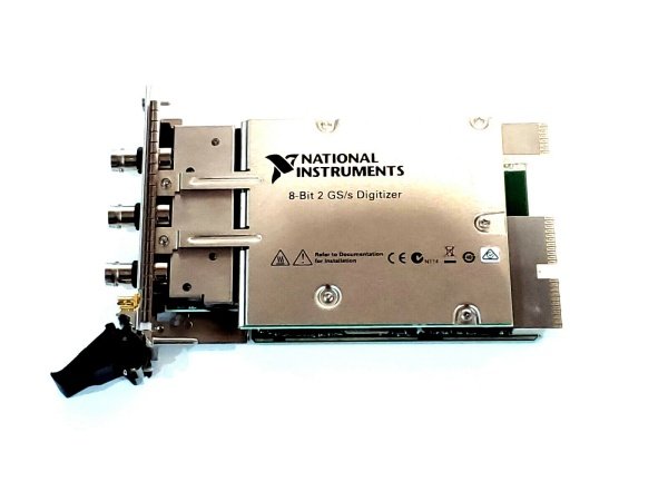
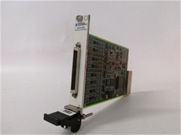
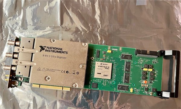
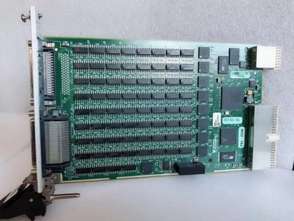
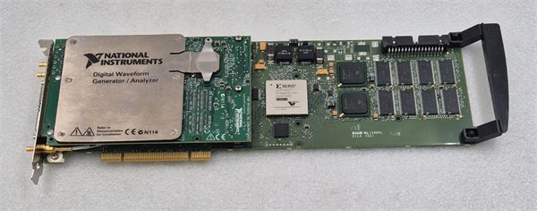
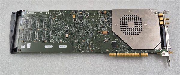
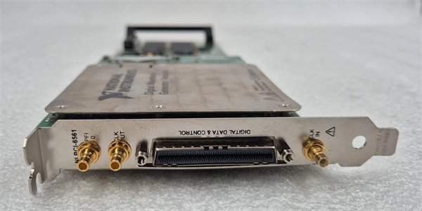
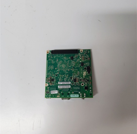
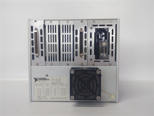
NI PCI-6561 High-Speed Digital Waveform Generator/Analyzer
Manufacturer:NI
Product Number:NI PCI-6561
Payment Methods:T/T, PayPal, Western Union
Condition:New & In Stock
Warranty:1 Year
Lead Time:1-3 Working Days
Certificate:COO
Courier partners:DHL, UPS, TNT, FedEx and EMS.
Business hours:7*24
Product Description
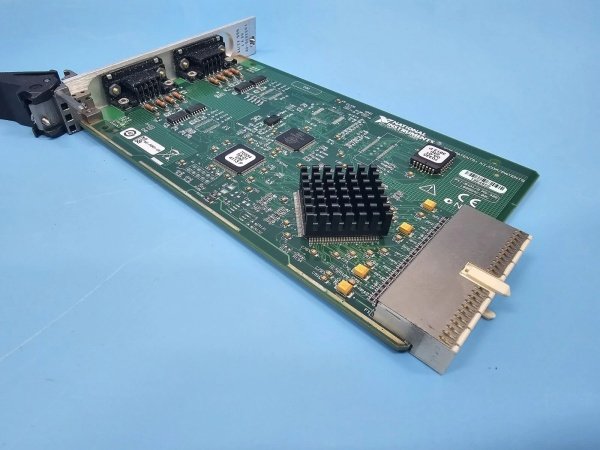
The NI PCI-6561 is a high-speed digital waveform generator/analyzer developed by National Instruments (NI), belonging to NI’s High-Speed Digital (HSD) product series—designed specifically for testing and validating high-speed digital interfaces in industrial automation and aerospace/defense systems. Unlike standard digital I/O cards (e.g., the NI PCI-6541), the NI PCI-6561 integrates dual functionality: it generates precise digital waveforms (up to 1.25 Gbps) for stimulating devices under test (DUTs) and analyzes received signals to verify performance—making it a all-in-one solution for high-speed protocol testing (e.g., PCIe, Ethernet, and SerDes).
In automation systems, the NI PCI-6561 acts as a “digital signal hub” for high-speed component validation. For example, in a data center switch test setup, it generates 10 Gbps Ethernet test frames to stress-test the switch’s ports, then analyzes the switch’s output signals to measure jitter, bit error rate (BER), and signal integrity. Its 256 MB onboard memory per channel stores long-duration test patterns (e.g., 10 million 64-bit data frames), enabling unattended testing—critical for validating the reliability of high-speed digital components in mass production.
Detailed parameter table
| Parameter name | Parameter value |
| Product model | NI PCI-6561 |
| Manufacturer | National Instruments (NI) |
| Product category | High-Speed Digital Waveform Generator/Analyzer (PCI Interface) |
| Electrical performance | 4 differential digital channels (8 single-ended); Logic levels: LVDS, LVPECL, TTL/CMOS (software-selectable); Maximum data rate: 1.25 Gbps per channel; Input/output voltage range: ±0.5 V (LVDS), 0–3.3 V (TTL) |
| Physical size | Dimensions (L×W×H): 175 mm × 106 mm × 25 mm (standard PCI form factor, with heatsink); Weight: Approximately 280 g |
| Interface type | PCI 2.3 compliant (32-bit, 33 MHz); 4 SMA connectors (for high-speed differential signals); 10-pin header (for trigger/synchronization); RTSI bus connector (8-line) |
| Communication protocol | PCI bus for data transfer; Compatible with NI-HSDIO driver; Supports DMA (direct memory access) for high-throughput data; Supports SCPI and LabVIEW FPGA programming |
| Environmental requirements | Operating temperature: 0 °C to 55 °C; Storage temperature: -20 °C to 70 °C; Relative humidity: 10% to 90% (non-condensing); Vibration resistance: 1.5 g (10 Hz to 500 Hz); Shock resistance: 30 g (11 ms half-sine) |
| Installation method | Standard PCI slot mounting (compatible with PCI 2.1/2.2/2.3 chassis); Requires dedicated heatsink contact (for thermal management); ESD protection (±15 kV air discharge) during installation |
| Performance indicators | Onboard memory: 256 MB per channel (for waveform storage); Signal jitter: < 50 ps (rms); Eye diagram analysis: Built-in (supports mask testing); Synchronization accuracy: ±10 ps across multiple cards |
| Power requirements | Powered by PCI bus + external 12 VDC power supply (for high-speed circuits); Typical power consumption: 15 W; Peak power consumption: 22 W (during 1.25 Gbps operation) |
| Compatibility |
Supported OS: Windows 10/11 (64-bit); Compatible software: NI LabVIEW, LabVIEW FPGA, C/C++,.NET; Works with NI TestStand for test sequence automation |
Core advantages and technical highlights
Multi-Protocol Support & Flexible Logic Levels: The NI PCI-6561 supports multiple high-speed logic standards (LVDS, LVPECL, TTL/CMOS) via software configuration, eliminating the need for external signal converters. For instance, when testing a mixed-signal PCB, it can generate LVDS signals (for high-speed data paths) and TTL signals (for control lines) simultaneously—adapting to diverse DUT interfaces without hardware reconfiguration. This flexibility reduces test setup time by 50% compared to single-standard tools.
Ultra-Low Jitter & High Signal Integrity: With signal jitter as low as 50 ps (rms), the NI PCI-6561 generates near-ideal digital waveforms—essential for testing sensitive high-speed components (e.g., 5G RF transceivers and aerospace-grade FPGAs). Its built-in eye diagram analysis tool visualizes signal quality in real time, allowing engineers to quickly identify issues like inter-symbol interference (ISI) or crosstalk. For example, when validating a SerDes link, the NI PCI-6561 measures the eye opening at different voltages and timings to ensure compliance with industry standards (e.g., IEEE 802.3bj for 100 Gbps Ethernet).
Scalable Synchronization & FPGA Programmability: The NI PCI-6561 supports RTSI bus synchronization, enabling multi-card setups (up to 8 cards) with ±10 ps timing alignment—critical for testing multi-lane high-speed interfaces (e.g., 4-lane PCIe Gen 3). Additionally, it integrates an FPGA (Xilinx Kintex-7) that users can program via LabVIEW FPGA to implement custom test logic (e.g., proprietary protocol decoding or real-time BER calculation). This programmability lets the NI PCI-6561 adapt to evolving standards (e.g., from 10 Gbps to 25 Gbps Ethernet) without hardware replacement.
Typical application scenarios
In aerospace/defense, the NI PCI-6561 is widely used for testing avionics high-speed data buses (e.g., ARINC 818 and Fibre Channel). For example, in a military aircraft’s mission computer test rig, the NI PCI-6561 generates ARINC 818 video data streams (up to 3 Gbps) to simulate camera inputs, then analyzes the computer’s output signals to verify data integrity—ensuring no frame loss or corruption during flight. Its ultra-low jitter (< 50 ps) mimics real-world avionics signal conditions, while the built-in eye diagram tool validates compliance with strict military standards (e.g., MIL-STD-1553).
In semiconductor manufacturing, the NI PCI-6561 validates high-speed I/O ports on advanced microchips (e.g., AI accelerators with PCIe Gen 4 interfaces). It generates PCIe test packets (up to 8 Gbps) to stress the chip’s I/O circuits, then measures BER and jitter to quantify performance. The NI PCI-6561’s 256 MB onboard memory stores complex test patterns (e.g., worst-case traffic scenarios), enabling 24/7 unattended testing of 1,000+ chips per day—helping semiconductor fabs reduce test costs by 30% compared to manual testing.
Installation, commissioning and maintenance instructions
Installation preparation: Before installing the NI PCI-6561, power off the industrial PC and confirm an empty PCI 2.1/2.2/2.3 slot with adjacent space for the heatsink. Wear an ESD wristband (rated ±15 kV) and use a grounded workbench to avoid damaging the card’s high-speed circuits. Connect the external 12 VDC power supply (provided by NI) to the card’s power connector—ensure the voltage polarity is correct (reverse polarity may damage components). Insert the NI PCI-6561 into the PCI slot until fully seated, then secure it with a chassis screw. Connect SMA cables (50 Ω impedance-matched) to the signal ports—use shielded cables to minimize EMI interference. Download and install the latest NI-HSDIO driver and LabVIEW FPGA, then use NI Measurement & Automation Explorer (MAX) to detect the NI PCI-6561 and run a self-test (includes jitter measurement and waveform generation verification).
Maintenance suggestions: Inspect the NI PCI-6561’s SMA connectors and heatsink monthly—clean SMA contacts with isopropyl alcohol (99.9% purity) and a lint-free cloth to remove oxidation, and ensure the heatsink is free of dust (use compressed air to clean). Calibrate the card annually using NI’s calibration kit (e.g., NI 9189) to maintain jitter accuracy and signal level precision. If the NI PCI-6561 fails to generate/analyze signals, check the external power supply (ensure 12 VDC ±5% stability) and reinstall the NI-HSDIO driver. Replace the card’s thermal paste (on the heatsink) every 2 years to maintain thermal performance—use NI-approved thermal compound (thermal conductivity ≥ 4 W/mK) to prevent overheating. Avoid exposing the NI PCI-6561 to temperatures above 55 °C or humidity above 90% to prevent degradation of high-speed components.
 Loading comments...
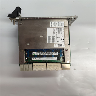
NI PCI-6561 High-Speed Digital Waveform Generator/Analyzer
Manufacturer:NI
Product Number:NI PCI-6561
Payment Methods:T/T, PayPal, Western Union
Condition:New & In Stock
Warranty:1 Year
Lead Time:1-3 Working Days
Certificate:COO
Courier partners:DHL, UPS, TNT, FedEx and EMS.
Business hours:7*24
Product Description
The NI PCI-6561 is a high-speed digital waveform generator/analyzer developed by National Instruments (NI), belonging to NI’s High-Speed Digital (HSD) product series—designed specifically for testing and validating high-speed digital interfaces in industrial automation and aerospace/defense systems. Unlike standard digital I/O cards (e.g., the NI PCI-6541), the NI PCI-6561 integrates dual functionality: it generates precise digital waveforms (up to 1.25 Gbps) for stimulating devices under test (DUTs) and analyzes received signals to verify performance—making it a all-in-one solution for high-speed protocol testing (e.g., PCIe, Ethernet, and SerDes).
In automation systems, the NI PCI-6561 acts as a “digital signal hub” for high-speed component validation. For example, in a data center switch test setup, it generates 10 Gbps Ethernet test frames to stress-test the switch’s ports, then analyzes the switch’s output signals to measure jitter, bit error rate (BER), and signal integrity. Its 256 MB onboard memory per channel stores long-duration test patterns (e.g., 10 million 64-bit data frames), enabling unattended testing—critical for validating the reliability of high-speed digital components in mass production.
Detailed parameter table
| Parameter name | Parameter value |
| Product model | NI PCI-6561 |
| Manufacturer | National Instruments (NI) |
| Product category | High-Speed Digital Waveform Generator/Analyzer (PCI Interface) |
| Electrical performance | 4 differential digital channels (8 single-ended); Logic levels: LVDS, LVPECL, TTL/CMOS (software-selectable); Maximum data rate: 1.25 Gbps per channel; Input/output voltage range: ±0.5 V (LVDS), 0–3.3 V (TTL) |
| Physical size | Dimensions (L×W×H): 175 mm × 106 mm × 25 mm (standard PCI form factor, with heatsink); Weight: Approximately 280 g |
| Interface type | PCI 2.3 compliant (32-bit, 33 MHz); 4 SMA connectors (for high-speed differential signals); 10-pin header (for trigger/synchronization); RTSI bus connector (8-line) |
| Communication protocol | PCI bus for data transfer; Compatible with NI-HSDIO driver; Supports DMA (direct memory access) for high-throughput data; Supports SCPI and LabVIEW FPGA programming |
| Environmental requirements | Operating temperature: 0 °C to 55 °C; Storage temperature: -20 °C to 70 °C; Relative humidity: 10% to 90% (non-condensing); Vibration resistance: 1.5 g (10 Hz to 500 Hz); Shock resistance: 30 g (11 ms half-sine) |
| Installation method | Standard PCI slot mounting (compatible with PCI 2.1/2.2/2.3 chassis); Requires dedicated heatsink contact (for thermal management); ESD protection (±15 kV air discharge) during installation |
| Performance indicators | Onboard memory: 256 MB per channel (for waveform storage); Signal jitter: < 50 ps (rms); Eye diagram analysis: Built-in (supports mask testing); Synchronization accuracy: ±10 ps across multiple cards |
| Power requirements | Powered by PCI bus + external 12 VDC power supply (for high-speed circuits); Typical power consumption: 15 W; Peak power consumption: 22 W (during 1.25 Gbps operation) |
| Compatibility |
Supported OS: Windows 10/11 (64-bit); Compatible software: NI LabVIEW, LabVIEW FPGA, C/C++,.NET; Works with NI TestStand for test sequence automation |
Core advantages and technical highlights
Multi-Protocol Support & Flexible Logic Levels: The NI PCI-6561 supports multiple high-speed logic standards (LVDS, LVPECL, TTL/CMOS) via software configuration, eliminating the need for external signal converters. For instance, when testing a mixed-signal PCB, it can generate LVDS signals (for high-speed data paths) and TTL signals (for control lines) simultaneously—adapting to diverse DUT interfaces without hardware reconfiguration. This flexibility reduces test setup time by 50% compared to single-standard tools.
Ultra-Low Jitter & High Signal Integrity: With signal jitter as low as 50 ps (rms), the NI PCI-6561 generates near-ideal digital waveforms—essential for testing sensitive high-speed components (e.g., 5G RF transceivers and aerospace-grade FPGAs). Its built-in eye diagram analysis tool visualizes signal quality in real time, allowing engineers to quickly identify issues like inter-symbol interference (ISI) or crosstalk. For example, when validating a SerDes link, the NI PCI-6561 measures the eye opening at different voltages and timings to ensure compliance with industry standards (e.g., IEEE 802.3bj for 100 Gbps Ethernet).
Scalable Synchronization & FPGA Programmability: The NI PCI-6561 supports RTSI bus synchronization, enabling multi-card setups (up to 8 cards) with ±10 ps timing alignment—critical for testing multi-lane high-speed interfaces (e.g., 4-lane PCIe Gen 3). Additionally, it integrates an FPGA (Xilinx Kintex-7) that users can program via LabVIEW FPGA to implement custom test logic (e.g., proprietary protocol decoding or real-time BER calculation). This programmability lets the NI PCI-6561 adapt to evolving standards (e.g., from 10 Gbps to 25 Gbps Ethernet) without hardware replacement.
Typical application scenarios
In aerospace/defense, the NI PCI-6561 is widely used for testing avionics high-speed data buses (e.g., ARINC 818 and Fibre Channel). For example, in a military aircraft’s mission computer test rig, the NI PCI-6561 generates ARINC 818 video data streams (up to 3 Gbps) to simulate camera inputs, then analyzes the computer’s output signals to verify data integrity—ensuring no frame loss or corruption during flight. Its ultra-low jitter (< 50 ps) mimics real-world avionics signal conditions, while the built-in eye diagram tool validates compliance with strict military standards (e.g., MIL-STD-1553).
In semiconductor manufacturing, the NI PCI-6561 validates high-speed I/O ports on advanced microchips (e.g., AI accelerators with PCIe Gen 4 interfaces). It generates PCIe test packets (up to 8 Gbps) to stress the chip’s I/O circuits, then measures BER and jitter to quantify performance. The NI PCI-6561’s 256 MB onboard memory stores complex test patterns (e.g., worst-case traffic scenarios), enabling 24/7 unattended testing of 1,000+ chips per day—helping semiconductor fabs reduce test costs by 30% compared to manual testing.
Installation, commissioning and maintenance instructions
Installation preparation: Before installing the NI PCI-6561, power off the industrial PC and confirm an empty PCI 2.1/2.2/2.3 slot with adjacent space for the heatsink. Wear an ESD wristband (rated ±15 kV) and use a grounded workbench to avoid damaging the card’s high-speed circuits. Connect the external 12 VDC power supply (provided by NI) to the card’s power connector—ensure the voltage polarity is correct (reverse polarity may damage components). Insert the NI PCI-6561 into the PCI slot until fully seated, then secure it with a chassis screw. Connect SMA cables (50 Ω impedance-matched) to the signal ports—use shielded cables to minimize EMI interference. Download and install the latest NI-HSDIO driver and LabVIEW FPGA, then use NI Measurement & Automation Explorer (MAX) to detect the NI PCI-6561 and run a self-test (includes jitter measurement and waveform generation verification).
Maintenance suggestions: Inspect the NI PCI-6561’s SMA connectors and heatsink monthly—clean SMA contacts with isopropyl alcohol (99.9% purity) and a lint-free cloth to remove oxidation, and ensure the heatsink is free of dust (use compressed air to clean). Calibrate the card annually using NI’s calibration kit (e.g., NI 9189) to maintain jitter accuracy and signal level precision. If the NI PCI-6561 fails to generate/analyze signals, check the external power supply (ensure 12 VDC ±5% stability) and reinstall the NI-HSDIO driver. Replace the card’s thermal paste (on the heatsink) every 2 years to maintain thermal performance—use NI-approved thermal compound (thermal conductivity ≥ 4 W/mK) to prevent overheating. Avoid exposing the NI PCI-6561 to temperatures above 55 °C or humidity above 90% to prevent degradation of high-speed components.
Need a Custom Automation Solution?
Our team of experts can design and implement a tailored automation system to meet your specific requirements.